
Mitsubishi Electric Corporation has announced its achievement of a world record photoelectric conversion efficiency rate of 18.6 percent in a 150-millimeter square practical use multi-crystalline silicon solar cell, an improvement of 0.6 percent over the company's previous record.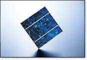
Background and Purpose of Development
Production volumes of solar, or photovoltaic (PV), systems have been increasing as they have garnered attention as a good source of renewable energy, against the background of increased global environmental awareness. While silicon is an essential component in the wafers used to make solar cells, the supply of silicon has not been able to keep up with demand. This is driving research into the development of thinner wafers that not only use less silicon, but also have improved efficiency and increased electrical output.
In a 150-millimeter square practical-use multi-crystalline silicon solar cell, Mitsubishi Electric has achieved the world's highest conversion efficiency rate of 18.6 percent by adding a low reflectivity surface texture on the multi-crystalline silicon wafer, by optimizing the p-n junction to increase electric current generation and by developing a process to print electrodes on the surface of the silicon (metallization) to reduce shade loss of front grid electrodes. This technology contributes to higher efficiency in small installations such as narrow roofs.
Main Features of the Newly Developed PV Cell
1) World's first developed with a low-reflective honeycomb textured structure, with a view to using the technology in next-generation high-efficient PV cells
To create highly efficient PV cells, it is necessary to reduce light reflectivity on the surface. While a honeycomb-textured structure is recognized as suitable for reducing surface reflectivity, it was a challenge to develop a way to apply this technology in production lines. Mitsubishi Electric has developed the world's first method for fabricating a honeycomb structure on the surface of a 150-millimeter square multi-crystalline silicon by combining laser patterning and wet etching.
2) Reduced emitter loss by optimizing the n-layer in p-n junction
Power generation also relies on the amount of light that approaches the p-n junction. A shallow, lightly doped emitter (n-layer) increases light gain and improves efficiency of power generation.
3) 25-percent reduced shade loss from front grid electrodes and larger effective electrical output surface area
With modified screens and front metal electrodes, Mitsubishi Electric reduced shading loss of front grid electrodes by 25 percent compared to previous cells.
Future Developments
Mitsubishi Electric will begin introducing this multi-crystal silicon cell technology into its mass-produced photovoltaic modules by fiscal 2011 (April 1, 2010-March 31, 2011).
Mitsubishi Electric also aims to increase output of solar power generation systems by combining this technology with its PV inverters, which have the industry's highest energy conversion efficiency rate. The company will promote these PV systems worldwide, thus contributing to environmental preservation and achieving a sustainable society.
The company plans to make a presentation of this achievement at "The 23rd European Photovoltaic Conference" in September 2008 in Spain.
