
Nanochip, Inc., a Silicon Valley startup, has managed to raise $14 million in funding from Intel Capital, Intel's global investment organization, for further development of the MEMS technology.You read it right: gigabytes, not gigabits. According to Nanochip, the technology isn't lithography constrained, allowing production of chips of more than 1GB in capacity, in plants that have already been deemed outdated by current standards. The lack of lithography constraints means cheaper products, resulting in an opportunity to also replace flash memory, as the technology is also non-volatile.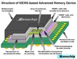
Today's factories should be able to produce the first products, estimated at 100GB per chip, when the technology is expected to be unleashed for public consumption by 2010. The first samples will be available during 2009.
PRAM or phase change memory was expected to be the technology to replace flash in the coming years, since it is also non-volatile, while it is much faster than flash. PRAM, though, doesn't seemed to scale so well, in regards to density, and still has some boundaries to overcome, namely it's thermal principles of operation.
Nanochip is using some kind hybrid PRAM technology in it's MEMS technology, although we don't know, yet, what this means in practical terms - it could mean a fast access speed. Access speed is a place where PRAM is appointed to be the undisputed king of the hill, so it could limit applications of this type of technology. The density claim seems to be right on since 1Tb is approximately 116GiB.
For now it seems that the flash SSD drives are going to be replaced before they even reach mass consumption - which is a good thing. The technology is expensive, doesn't provide a lot of storage space and is prone to failure, due to the low amount of write cycles available per cell. Flash is perfect for pendrives and resisting shock, not so good for regular, intensive, HDD usage.
